We complete our clock module by adding a halt signal and test it with our address register. Now our (future) programs won’t have to run forever.
Schematic:

- note: schematic has been updated with changes from logic families video
Transcript:
In this series we’re building a homebrew CPU, and so far we’ve built an address register, and we’ve almost completed our clock module.
The last feature our clock module needs is a halt signal, and this is kind of exciting because it’s the first time we’re adding feedback between the modules.
Feedback allows for more complex systems and eventually Turing-completeness. Now, we’ve got a long ways to go before we’re computing anything, but this halt signal will allow us to create programs that have an ending
instead of just running until we shut the power off.
So what does a halt signal look like? Normally the halt signal will be low and our clock will be running and advancing our address register.
When the halt signal goes high however, the clock will stop.
First notice that we have an inverse reset pin on our 555 timer.
This is the perfect way to stop the clock.
When it’s high the clock is running and when it’s low the clock is stopped.
So one inverter and we’re done?
This is where the feedback comes in.
The clock drives the rest of the CPU but the CPU tells the clock when to stop.
There’s an interesting problem here.
What if the CPU starts in a state where it’s telling the clock to halt?
Nothing will ever happen. The program won’t start.
In the last video we built a reset circuit that comes on automatically at power on.
If the reset can be allowed to make the clock run even when halt is high then we won’t be stuck.
This will also mean we can use the new reset button to restart a halted program, and that’s pretty handy.
This sounds like some more digital logic.
The clock runs when reset is high or when the halt signal is low.
If we use an OR gate to implement this logic it will look like this.
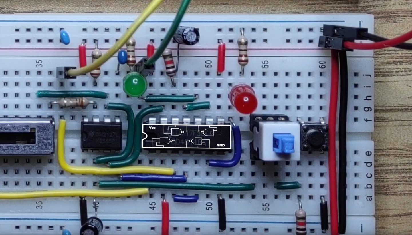
We need an inverter for the halt signal and one OR gate.
We saw in the last video that we can use a NAND gate to make an inverter
and we have one of those left over.
So that means we need just one more chip to implement our halt logic, right?
What if we could do better than that?
We have one NAND gate remaining.
This is the logic table for a NAND gate.
It has three high outputs just like an OR gate.
If we connect the halt signal to one input
we can see we need an inverted reset signal as the other input
to get our desired output.
Well look at that.
We have an inverted reset right here that we use to drive the inverted reset on our counters.
That means we should be able to add a halt signal with no additional chips.
So let’s do that.
Disconnect 5 volts from the inverse reset pin on the 555 timer and connect it to our NAND gate output instead.
Connect our inverse reset to one input.
The other input is our halt signal.
Use a red LED to show the state.
Connect our halt signal to zero volts for now.
When we bring halt high the clock stops.
There’s something satisfying about minimizing parts like this.
our one quad NAND gate chip is providing a delayed initial clock, an inverse clock, an inverse reset and halt functionality.
If that’s not exciting, instead of minimizing parts
we could be optimizing for simplicity, or performance, or features.
There really are endless puzzles to solve when designing electronics projects like this.
Let’s connect our halt signal to bit 9 of our address register.
Reset starts our addresses counting again.
Once bit 9 is set the clock stops again.
We can connect halt to one of the terminal count outputs. This should stop the clock when all the bits to the right are “1”.
Had some power distribution issues. Moving the power connector seems to have helped.
With the halt signal on bit 13 our address will count from 0 to 8192 and stop.
When we build more of the CPU we could add a control line and a halt instruction or we could add a jump instruction and use bit 15 of the address register.
For now our clock module is complete.
In the next video we’ll see how to read values from our EEPROM using our address register.
I hope you enjoyed this video. See you next time.