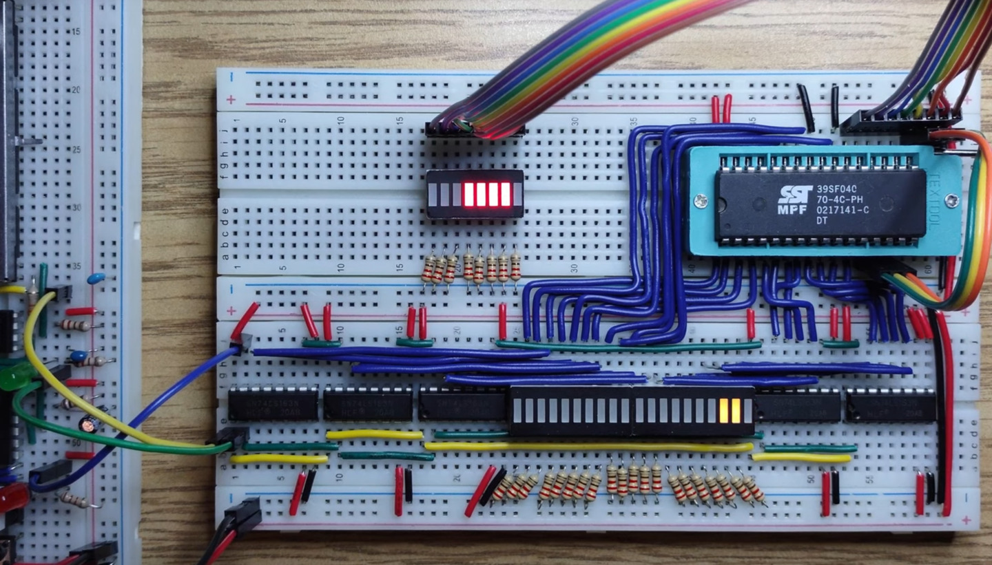
We build a larger address register and use it to test an SST39SF040 512k flash chip.
Transcript:
In this series we’re building a homebrew CPU. Our plan was to use a 32k EEPROM in the build, but these parts are getting harder and harder to find. So instead let’s use this 512k SST39SF040 which is both cheaper and much easier to source. The 32k EEPROM has 15 address pins so we built a 16-bit address register. Our new flash chip has 19 address pins so let’s add another 4-bit 74LS163 to the register. Maybe here? We’ll squeeze it…
So today we’re building a 20-bit address register with five 74LS163 4-bit counters and two 10-segment led bar graphs.
In previous videos we covered how these 4-bit counters work together to create a larger register.
VCC to 5 volts. GND to 0 volts. Count enable parallel high.
Inverse reset connected together. Clock pins connected together.
Terminal count from one 74LS163 to count enable trickle on the next. This is what creates the larger register.
Inverse parallel load to 5 volts; for now all we need is counting, parallel load is for setting the values.
Now let’s bring all 20 output lines over to the LED bar graphs
and add current limiting resistors to zero volts.
Let’s check that this works.
We connect the clock line from our clock module.
We connect the reset line and let’s connect the halt line to the last terminal count.
Start the clock.
The low bits look good so far but this is a little slow to test the high bits,
so let’s use a smaller capacitor to increase the maximum clock rate. We’ll switch from a 10 microfarad to a 10 nanofarad. That should make our clock a thousand times faster, and 2 to the power of 10 is 1024 so bit 10 should now be changing about as fast as bit 0 was before. The count stops when all the bits are set which is 2 to the power of 20 minus 1.
Let’s put the 10 microfarad capacitor back.
Now we can connect the flash to our address register.
You can see there’s a lot of pins on this chip, and that just means lots of opportunity for bent pins. So if you can, and especially for chips like this where we’re going to be taking it out and putting it back in a lot, use a ZIF socket. ZIF stands for zero insertion force and it works by grabbing the edges of the pins instead of making you force them into something.
VDD to 5 volts. VSS to zero volts.
Inverse write enable high: we are only going to be reading data.
Inverse output low: always output.
Inverse chip enable low as well
A0 through A3 to the first counter.
A4 through A7 to the second counter.
The address numbering jumps around a bit from here. A12, A15 A16 A18 to the address display.
A17, A14, A13 around the top.
And A8 through A11 are the last address pins.
Let’s connect the data pins to an LED bar graph.
D0 through D2 on one side.
D3 through D7 on the other.
Now we can start the clock and see the contents of the flash memory. The flash has some simple repeating patterns programmed into it.
We can see those patterns now on the data display.
In this series we’re building a CPU just capable of playing some simple games. If, like me, you’re easily amused you might say that this already qualifies. See, we can use the clock control to try stopping the display when no bits are set.
And that’s fun for a little while, but we have bigger plans and this doesn’t even qualify as a CPU yet.
In this video we built a new address register and used it to read from a 512k flash chip. In the next video we will connect the flash to an LCD display to playback something a little more interesting.
I hope you liked this video. See you next time.